Thermal Imaging Solutions for Semiconductor Manufacturing, Monitoring and R&D


Semiconductor manufacturing, equipment maintenance and device development require different kinds of temperature information. Non-contact infrared imaging can reveal surface temperature patterns that help teams investigate abnormal heating, monitor operating conditions and evaluate thermal behavior. The appropriate imaging approach depends on whether the task is a portable inspection, ongoing equipment or process monitoring, or controlled research and development (R&D) analysis.
The need for reliable thermal information extends from tightly packed chip and board assemblies to the equipment that supports fabrication. Components with different power and cooling characteristics can develop unusual heat patterns associated with excessive loading, inadequate heat dissipation or electrical faults. In production, abnormal temperatures on accessible chambers, pumps, cooling lines or electrical systems may also signal conditions that warrant further investigation.
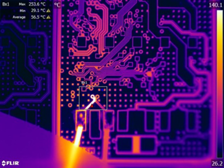
Unlike contact probes, infrared imaging captures a two-dimensional temperature pattern without touching the target. It can support quick comparisons between similar devices, between locations on the same board, or against a previously established reference image. Thermal cameras measure apparent surface temperature; correct interpretation depends on emissivity, reflections, viewing geometry and operating conditions.
Maintenance teams can screen accessible exterior surfaces of etching, deposition (CVD/PVD) and rapid thermal processing equipment, including chamber walls, heating assemblies and cooling pipelines. Unusual surface temperature patterns may help flag insulation problems, local heating irregularities or changes in cooling performance. Thermal imaging does not directly measure conditions inside a closed process chamber.
Surface scans of vacuum pumps, motors, bearings, flanges and associated pipework can highlight abnormal heating or temperature differences for follow-up inspection. Thermal signatures may be consistent with mechanical friction, heat leakage or cooling problems, but should be interpreted alongside maintenance data and other diagnostic measurements.
Thermal inspections can help identify overheating in accessible electrical cabinets, drive power supplies, RF power modules and UPS connections. Teams may also scan equipment cooling ducts and chiller-related surfaces serving lithography or metrology systems. Inspections must follow electrical safety and site cleanroom procedures.

Electric fuses heating up from being under load.
After power-on, engineers can inspect the surface temperature distribution of circuit boards and packaged devices, including power-management ICs, memory, interface ICs and other components. Unexpected hot spots can help prioritize investigation of suspected short circuits, leakage paths, excessive power dissipation or poor thermal contact. A hot spot is a screening clue, not by itself proof of a particular defect.
Thermal images can be compared across known-good and suspect assemblies to identify deviations in package surface temperature. This can support preliminary sorting during validation, burn-in or aging checks, provided that the devices are tested under comparable loads and ambient conditions. Thermal results should be combined with electrical and quality tests before making accept/reject decisions.
In R&D and engineering validation, controlled thermal analysis helps characterize temperature distribution, heat dissipation and temperature rise in semiconductor devices, packages and circuit boards. Depending on the measurement objective, specialized laboratory cameras may be paired with close-up optics, high-speed acquisition or lock-in thermography to investigate localized heating, fast thermal transients and potential failure mechanisms. These are specialized R&D methods rather than ordinary continuous production-monitoring functions.
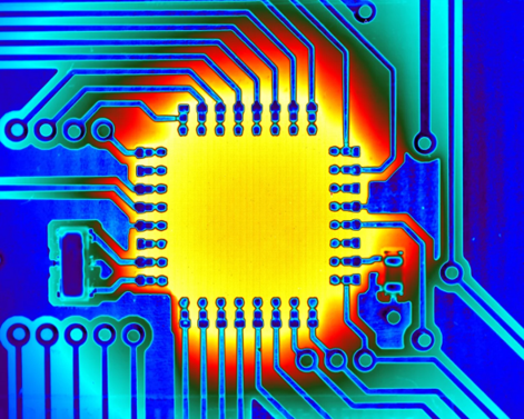
These findings must be interpreted within the limits of infrared measurement. Thermal imaging should not be assumed to reveal buried circuit defects directly, measure internal chamber temperatures through opaque walls or resolve microscopic structures without suitable optics and methods. Surface emissivity, reflections, viewing angle, enclosure materials and operating conditions affect interpretation. For concealed defects or highly localized phenomena, microscopic, lock-in or other specialized techniques may be more appropriate.
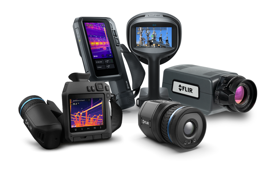
FLIR offers complementary approaches for different semiconductor needs. Handheld cameras help maintenance and engineering teams carry out scheduled inspections, investigate unexpected heating and screen accessible boards or packages. Fixed thermal monitoring solutions support repeated or continuous observation of selected manufacturing equipment and process surfaces, helping teams identify changes and plan follow-up action. For semiconductor R&D, specialized thermal imaging systems support device characterization, thermal design evaluation, high-speed measurements and advanced failure-analysis workflows when configured with the appropriate optics and methods.
Across these applications, thermal observations are most useful when interpreted alongside electrical tests, process records and other engineering evidence. The inspection or measurement method should be selected according to the target, operating conditions and level of detail required.
Explore how FLIR handheld inspection cameras, fixed monitoring solutions and specialized R&D thermal imaging systems can support semiconductor manufacturing and development. Contact a FLIR specialist to discuss your inspection, monitoring or thermal analysis requirements and identify an appropriate solution.
