FLIR Thermal Imaging Cameras Improve Reliability and Productivity of High-Performance Semiconductor Packaging Processes
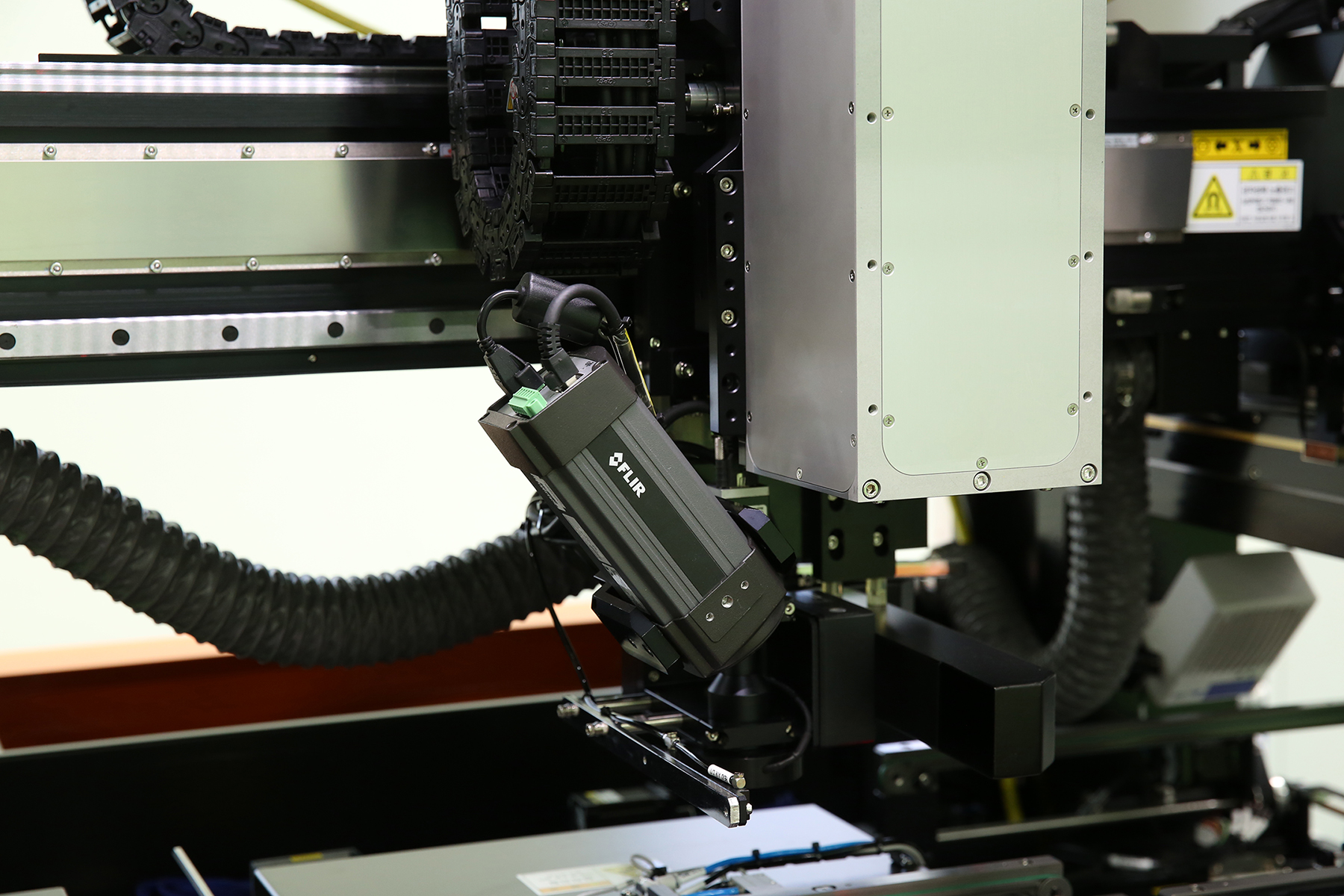
Integrating FLIR thermal imaging cameras with semiconductor packaging equipment has led to a dramatic increase in the reliability and productivity of manufacturing processes. Protec, a manufacturer of semiconductor post-processing equipment, introduced the FLIR A315 thermal imaging camera to the design of its Laser Assisted Bonding (LAB) equipment, a type of advanced packaging equipment for high-density, high-performance semiconductors such as flash memory and system LSI. The FLIR A315 is an effective solution for the precision temperature measurement requirements presented by lasers used as heat sources for LAB.
Protec, a company specialized in semiconductor post-processing equipment such as dispensers, die bonders, and pneumatic cylinders, has been supplying Laser Assisted Bonding (LAB) equipment to leading domestic and overseas semiconductor manufacturers and packaging companies since 2018. As its name suggests, LAB equipment uses lasers as a source of heat for bonding applications. Widely regarded as a type of next-generation technology, LAB not only dramatically increases manufacturing productivity and reliability compared to existing reflow soldering technologies, but also eliminates the disadvantages posed by conventional reflow soldering.

LAB technology eliminates the disadvantages posed by conventional reflow soldering
The traditional reflow soldering method uses hot air to raise the temperature of an entire oven room to 300°C. As such, it takes a few minutes for the heat to reach the target temperature, resulting in a slow soldering process. Reflow soldering also exposes parts that do not need soldering to heat, which presents a significant risk of deformation caused by thermal stress. Considering the latest trends in the semiconductor industry-such as using a thinner substrate or designing a smaller chip size as a means to deliver greater semiconductor performance and integration-reflow soldering increases the possibility of distortion caused by heat.
In contrast, LAB uses a laser beam to irradiate the required area/spot. Given the properties of lasers, it can reach the target temperature in seconds or even in milliseconds, reducing thermal stress. Moreover, LAB offers the advantage of greatly improving the units per hour (UPH) since it can process multiple products simultaneously in panel units. LAB clearly has multiple advantages over reflow soldering. However, in order to deploy LAB equipment, the target facility must have equipment capable of measuring the exact temperature of the laser and checking the overall distribution of heat.
“Earlier, we manufactured contact-type temperature kits with temperature sensors ourselves to measure temperature,” says Seok-Ji Im, Manager, CS Team, System Division III from Protec Co. Ltd “But these kits took a while to manufacture, and users had trouble reusing them multiple times. Later, we replaced our temperature sensors with short focal length infrared thermometers. However, this method was also limited in terms of the area we could measure and the wavebands we could use. Ultimately, we decided to upgrade to FLIR’s A315 thermal camera, and that helped us develop and mass produce our LAB equipment starting 2018.”
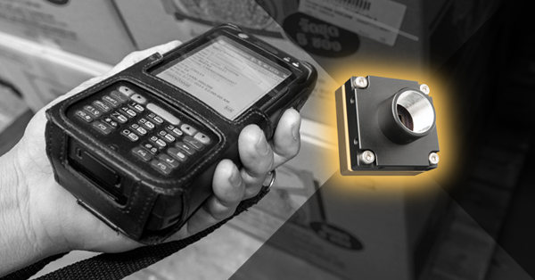
FLIR A315 measures up to 2,000°C, and supports 60 Hz full-frame streaming
Protec tested several other thermal camera models before settling on the FLIR A315, which provided the temperature measurement solutions required for deploying LAB equipment.
“In order to be integrated into our LAB equipment model engineered for mass production, the thermal camera had to be capable of producing highly accurate measurement results, and maintain this accuracy consistently throughout the entire testing period, which lasted at least six months,” says Im. “Not only that, the thermal camera for our LAB equipment had to support full-frame performance at 60Hz, and be reasonably competitive pricewise to make enough room for the mass production and manufacturing of the final product. The FLIR A315 proved to be a solution that satisfied all of these requirements.”
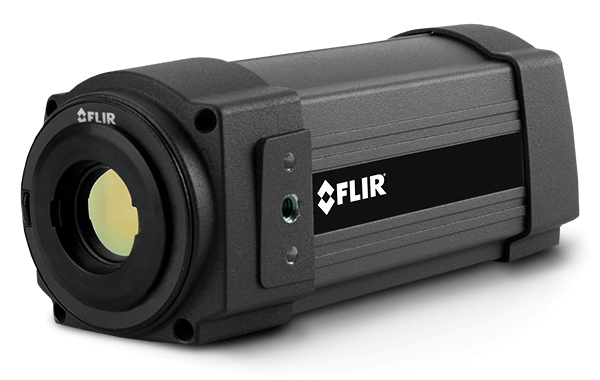
The FLIR A315 is a compact and economical thermal imaging camera that can be fully controlled using a computer. As it supports industry standard technology, the camera is compatible with third-party machine vision software (plug-and-play connection), including software from National Instruments, Cognex, Matrox, MVtec, and Steamer Imaging.
With a 320 × 240 (76,800) pixel microbolometer, the FLIR A315 can measure temperatures from 0 to 500°C (up to 2,000°C depending on the selected model), and detect minute differences in temperature (as little as 50 mK) even from a long distance. The FLIR A315 streams full-frame 16-bit images at 60 Hz while simultaneously transmitting signals, temperature linear data, and radiometric data.
FLIR thermal technology is essential in ensuring the reliability and productivity of LAB equipment
Young-Jun Son, Deputy General Manager, Sales Team, System Division III at Protec, explains the growing need for LAB equipment and the importance of FLIR thermal imaging for deploying it. “As electronic products become smaller in size,” he says, “and yet more impressive in terms of performance, semiconductor packaging technology is transitioning from traditional methods, such as the lead frame, to a chip scale package (CSP) or a flip chip method. In other words, semiconductor packaging technology is evolving such that it is possible to reduce the packaging size to a point where the packaging is as small as the chip itself, or improve processing speed.”
“In line with the continued evolution of packaging technology,” he adds, “the demand for LAB equipment is expected to rise, and thermal imaging camera equipment such as the FLIR A315 is essential to ensure the reliability and productivity of LAB equipment.”
Protec’s LAB equipment can be used for various applications, such as display, PCB systems on package, (SoP), as well as semiconductor packaging processes that are currently being supplied to and used by customers.
Related Articles
-
 Application Story
FLIR cameras support analysis and diagnosis of external thermal insulation systems
Read the Story -
 Case Study
Automatic Health Check in Dairy Farms Using FLIR Thermal Imaging Cameras
Read the Story -
 Deep Learning
Comparing Deep Learning Cameras with Smart Cameras
Read the Story