Using PPS to Synchronize with External GPS
Supported Products
Ladybug5+
Ladybug6
Overview
Pulse per second (PPS) is a common feature in GPS units and IMUs to provide an accurate timing signal to assist with precision synchronization of various devices to a common clock. It is commonly provided as a TTL signal at either 3.3 V or 5 V.
The Ladybug is able to directly accept PPS signals and NMEA data streams over the GPIO pins. This allows the Ladybug to maintain an internal precision time that is continuously synchronized with GPS time. Therefore, the timestamps attached to each image frame may be considered to be within microseconds of GPS time. The Ladybug does not process or output GPS positioning data.
The Ladybug cannot accept an RS232 signal from the GPS device. If your signal is RS232, you need to convert it to TTL for use with this feature.
Note: The Ladybug library has the ability to interface with a GPS device and insert NMEA sentence data into Ladybug images. The data can then be extracted at a later time and be used to generate HTML data, which can be displayed as a Google Map, or KML data, which can be loaded into Google Earth. For information on how to use this feature see Using an External GPS Device with Ladybug Cameras.
Test configuration
| Item | Description |
|---|---|
| Camera | Ladybug6 |
| Firmware | 1.0.13.2 |
| Software | LadybugCapPro 1.17.0.268 |
Technical notes
Data formats supported
The camera supports the following NMEA sentence types:
- GGA—fix information. This is required with either of the following:
- ZDA—date and time
- RMC—recommended minimum data for GPS
Timestamp
The LadybugImageInfo contains the timestamp and shutter time information.
In trigger mode, the GPS timestamp is stored at the end of integration. The timestamp accuracy has a positive offset of 45 μs ±8 μs.
In free running mode, the GPS timestamp is stored at the start of integration.
To calculate the mid point of a frame's timestamp:
Mid Point = Timestamp - 45 μs - 0.5 x Shutter Time
GPIO pin assignments
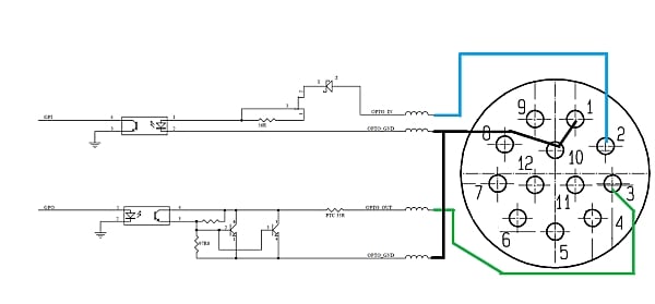
The GPIO pin 4 IO2 is used for GPS data.
The GPIO pin 11 IO3 is used for PPS signal, active on low to high transition.
The GPIO pin 12 is used as a signal ground for IO2 and IO3.
The camera has a 12-pin GPIO connector on the bottom of the case; refer to the diagram below for wire color coding. The GPIO is a Hirose waterproof 12-pin female connector (Mfg P/N:LF10WBP-12SD).
| Diagram | Color | Pin | Function | Description |
|---|---|---|---|---|
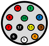 |
Green | 1 | OPTO_GND | Ground for opto-isolated IO pins |
| Blue | 2 | I0 | Opto-isolated input (default Trigger in) | |
| Brown | 3 | O1 | Opto-isolated output | |
| Orange | 4 | IO2 | Input/Output / GPS data | |
| White | 5 | +3.3 V | Power external circuitry up to 150 mA | |
| Black | 6 | GND | Ground for bi-directional IO, VEXT, +3.3 V pins | |
| Red | 7 | VEXT | Allows the camera to be powered externally | |
| Red | 8 | VEXT | Allows the camera to be powered externally | |
| Red | 9 | VEXT | Allows the camera to be powered externally | |
| Green | 10 | OPTO_GND | Ground for opto-isolated IO pins | |
| Yellow | 11 | IO3 | Input/Output / PPS signal | |
| Black | 12 | GND | Ground for bi-directional IO, VEXT, +3.3 V pins |
Opto-isolated electrical characteristics
Values are for reference only and could vary between cameras.
| External Voltage |
External Resistor |
OPTO_OUT Low Voltage |
OPTO_OUT High Voltage |
Current |
|---|---|---|---|---|
| 3.3 V | 200 Ω | 1.44 V | 3.29 V | 8.2 mA |
| 5.0 V | 1.0 KΩ | 0.88 V | 4.94 V | 3.8 mA |
| 12 V | 2.0 KΩ | 1.1 V | 11.93 V | 5.1 mA |
| 12 V | 2.4 KΩ | 0.98 V | 11.93 V | 4.2 mA |
| 24 V | 4.7 KΩ | 0.75 V | 23.75 V | 4.5 mA |
Opto-isolated input output circuit
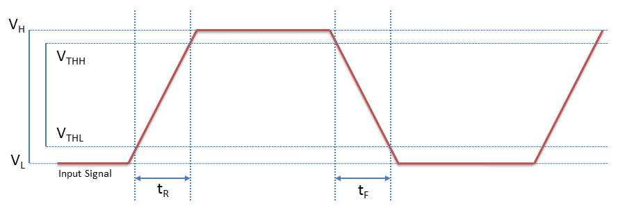
Opto-isolated input timing characteristics
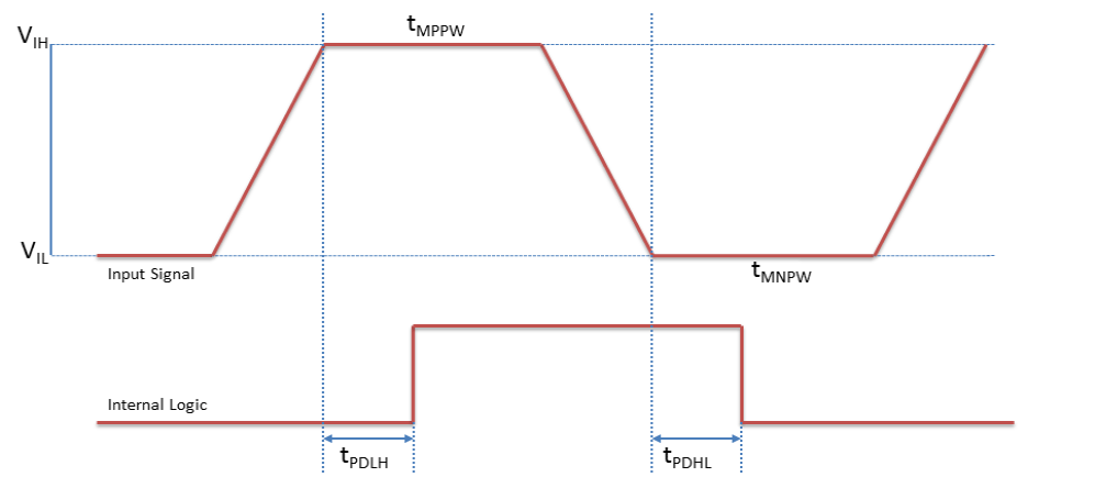
Opto-isolated input timing characteristics (5Vpp 1KHz Source Input)
Source
| Parameter | Symbol | Value |
| Input Low Voltage | VL | 0.03 V |
| Input High Voltage | VH | 4.69 V |
| Input Threshold High Voltage | VTHH | 4.22 V |
| Input Threshold Low Voltage | VTHL | 0.5 V |
| Cycle Rise Time | tR | 93.32 nS |
| Cycle Fall Time | tF> | 92.82 nS |
FPGA reads
| Parameter | Symbol | Value |
| Input Low Voltage | VL | 0.13 V |
| Input High Voltage | VH | 3.34 V |
| Input Threshold High Voltage | VTHH | 3.02 V |
| Input Threshold Low Voltage | VTHL | 0.45 V |
| Cycle Rise Time | tR | 17.74 µS |
| Cycle Fall Time | tF | 1 µS |
Triggering
| Parameter | Symbol | Opto-isolated |
| Propagation Delay Low to High (Source POV) | tPDLH | 556.98 nS |
| Propagation Delay High to Low (Source POV) | tPDHL | 26.4 µS |
| Minimum Positive Pulse Width (Input Source) | tMPPW | 56.5 µS |
| Minimum Negative Pulse Width (Input Source) | tMNPW | 2.16 µS |
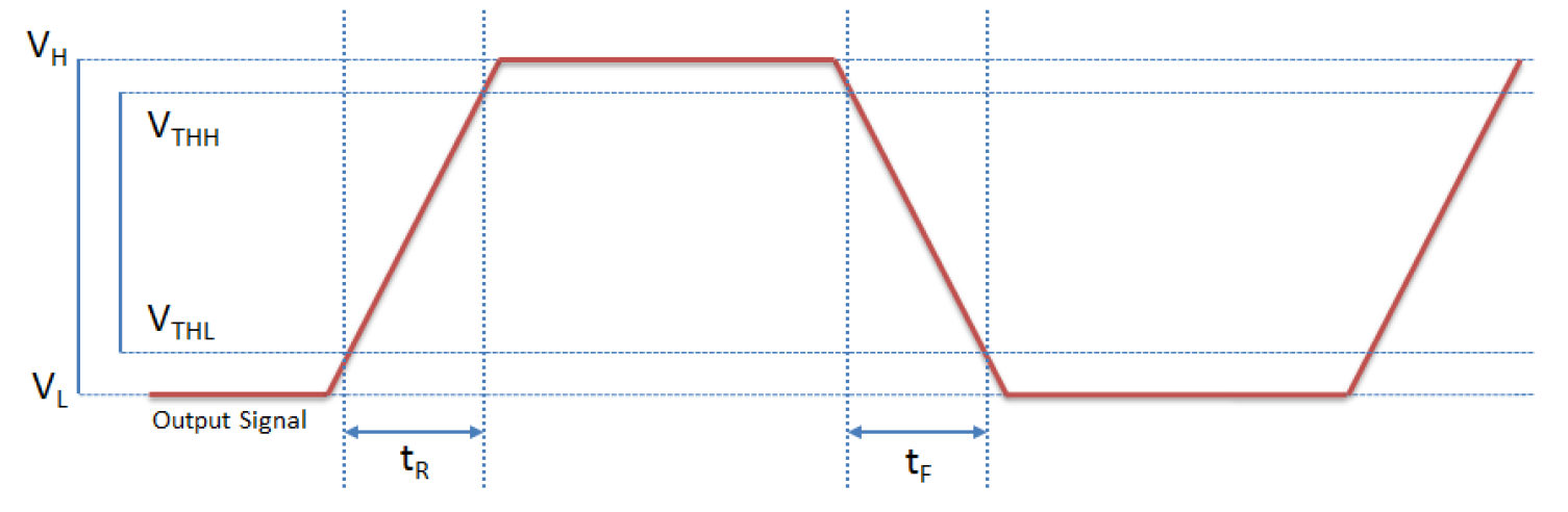
Opto-isolated output timing characteristics

Opto-isolated output performance at 7.5 FPS (measured with line pull up to Vcc = 5V, Rext = 1.0 KΩ)
| Parameter | Symbol | Opto-isolated |
| Output Low Voltage | VL | 0.84 V |
| Output High Voltage | VH | 5.06 V |
| Output Threshold High Voltage | VTHH | 4.64 V |
| Output Threshold Low Voltage | VTHL | 1.35 V |
| Cycle Rise Time | tR | 13.06 µS |
| Cycle Fall Time | tF | 2.63 µS |
| Opto Current (when triggering another camera) | 3.87 mA | |
| Opto Isolator Delay (High to Low) | 2.92 µS | |
| Opto Isolator Delay (Low to High) | 24.2 µS |
Non-isolated electrical characteristics
Values are for reference only and could vary between cameras.
Non-Isolated input and output GPIO circuit
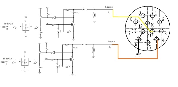
Non-isolated input timing characteristics
Input Performance (measured with a 3.3Vp-p 1KHz Square Wave input @ point A)
Input Source Pulse
| Parameter | Symbol | |
| Input Low Voltage | VL | 0.11 V |
| Input High Voltage | VH | 3.34 V |
| Input Threshold High Voltage (90%) | VTHH | 3.01 V |
| Input Threshold Low Voltage (10%) | VTHL | 0.43 V |
| Cycle Rise Time | tR | 154.9 nS |
| Cycle Fall Time | tF | 155.32 nS |
FPGA reads (measured at point B)
| Parameter | Symbol | |
| Input Low Voltage | VL | 0.6 V |
| Input High Voltage | VH | 2.84 V |
| Input Threshold High Voltage (90%) | VTHH | 2.62 V |
| Input Threshold Low Voltage (10%) | VTHL | 0.82 V |
| Cycle Rise Time | tR | 49.37 nS |
| Cycle Fall Time | tF | 71.12 nS |
Delays (Comparison between point A and point B)
| Parameter | Symbol | |
| Propagation Delay Low to High | tPDLH | 122.88 nS |
| Propagation Delay High to Low | tPDHL | 109.15 nS |
| Positive Pulse Width | tMPPW | 0.772 mS |
| Negative Pulse Width | tMNPW | 32.56 mS |
Minimums
| Parameter | Symbol | |
| Input High Voltage (point A) | VIH | ≥ 1.13 V |
| Propagation Delay Low to High (Between point A and point B) | tPDLH | 227.46 nS |
| Propagation Delay High to Low (Between point A and point B) |
tPDHL | 108.47 nS |
| Input Low Voltage (point A) | VIL | ≤ 1.73 V |
| Propagation Delay Low to High (Between point A and point B) | tPDLH | 101.72 nS |
| Propagation Delay High to Low (Between point A and point B) | tPDHL | 118.76 nS |
| Minimum Positive (on) Pulse Width (Input Source, point A) | tMPPW | 280 nS |
| Minimum Positive (on) Pulse Width (Camera receives, point B) | tMPPW | 365 nS |
| Minimum Negative (off) Pulse Width (Input Source, point A) | tMNPW | 620 nS |
| Minimum Negative (off) Pulse Width (Camera receives, point B) | tMNPW | 553.78 nS |
Non-isolated output timing characteristics
GP Output Performance @ Point A (Internal Vcc = 3.3V, Rext = 4.7 KΩ)
| Parameter | Symbol | |
| Output Low Voltage | VL | 0.08 V |
| Output High Voltage | VH | 3.12 V |
| Output Threshold High Voltage (90%) | VTHH | 2.82 V |
| Output Threshold Low Voltage (10%) | VTHL | 0.38 V |
| Cycle Rise Time | tR | 10.84 µS |
| Cycle Fall Time | tF | 1.08 µS |
GP Output Performance @ Point A (adding pull up to Vcc = 5V, Rext = 1 KΩ to the line)
| Parameter | Symbol | |
| Output Low Voltage | VL | 0.31 V |
| Output High Voltage | VH | 5.012 V |
| Output Threshold High Voltage (90%) | VTHH | 4.54 V |
| Output Threshold Low Voltage (10%) | VTHL | 0.78 V |
| Cycle Rise Time | tR | 1.99 µS |
| Cycle Fall Time | tF | 1.57 µS |
Configuring PPS/GPS synchronization
To configure time synchronization you must enable PPS and enable GPS time synchronization.
Using Ladybug API
There are two functions:
- ladybugSetGpsTimeSync()
- ladybugGetGpsTimeSync()
These take a camera context and a GpsTimeSyncSettings structure as follows:
- unsigned int baudRate
- bool enablePps
- bool enableGpsTimeSync
Using camera registers
| Offset | Name | Field | Bit | Description |
|---|---|---|---|---|
| 0x1EAC | PPS | Presence_Inq | [0] | Presence of the feature 0 = not available 1 = available |
| PPS_Inversion_Presence_Inq | [1] | Presence of the PPS Inversion Feature | ||
| [2-22] | Reserved | |||
| PPS_Inversion_Toggle | [23] | 0 = PPS low to high detect (default) 1 = PPS high to low detect |
||
| [24-30] | Reserved | |||
| PPS_Enable | [31] | Enable PPS 0 = disabled 1 = enabled |
| Offset | Name | Field | Bit | Description |
|---|---|---|---|---|
| 488h | SIO_CONTROL_CSR_INQ | SIO_Control_Quadlet_Offset | [0-31] | 32-bit offset of the SIO CSRs from the base address of initial register space |
| Base + 0h | SERIAL_MODE_REG | Baud_Rate | [0-7] | Baud rate setting 0 = 300 bps 1 = 600 bps 2 = 1200 bps 3 = 2400 bps 4 = 4800 bps 5 = 9600 bps (recommended) 6 = 19200 bps 7 = 38400 bps 8 = 57600 bps 9 = 115200 bps A = 230400 bps |
| Base + 4h | SERIAL_CONTROL_REG | RE | [0] | Enable receive Indicates if the camera's ability to receive data is enabled. Enabling this register causes the receive capability to be immediately started. Disabling this register flushes the the data in the buffer. 0 = disabled 1= enabled |
For a complete list of registers, see the Teledyne Machine Vision Camera Register Reference.
Verifying configuration
You can view the time synchronization status from the LadybugImageInfo:
- unsigned int ulGpsFixQuality
- bool bPpsStatus
- bool bGpsStatus
You can also verify the configuration using camera registers.
| Offset | Name | Field | Bit | Description |
|---|---|---|---|---|
| 0x1E9C | GPS_PPS_TIME_SYNC_VERIFICATION | Presence_Inq | [0] | Presence of the feature 0 = not available 1 = available |
| [1-23] | Reserved | |||
| GPS_Fix_Quality | [24-27] | Represents the quality setting from a GGA NMEA sentence | ||
| [28-29] | Reserved | |||
| GPS_Signal | [30] | GPS signal 0 = invalid 1 = valid |
||
| PPS_Signal | [31] | PPS signal 0 = invalid 1 = valid |
API Example
The API example ladybugGPSTimeSync demonstrates the configuration. The example is provided in the Ladybug SDK, available from the downloads page.